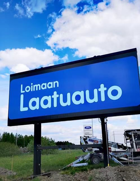
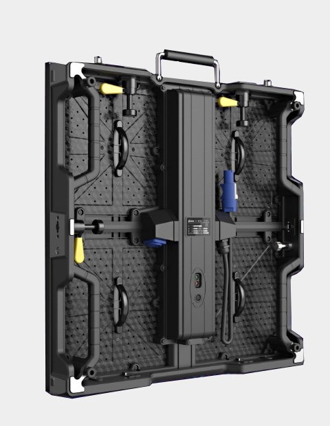
With the development of LED display screens, LED packaging technology is always indispensable. As two mainstream packaging solutions, COB and SMD technology are not only related to the distribution of interests in the upstream and downstream of the industrial chain, but also directly affect the user experience of end users. GDHANHENG used LED wall will conduct an in-depth analysis of these two packaging technologies from multiple dimensions.
Comparison of technical principles and production processes
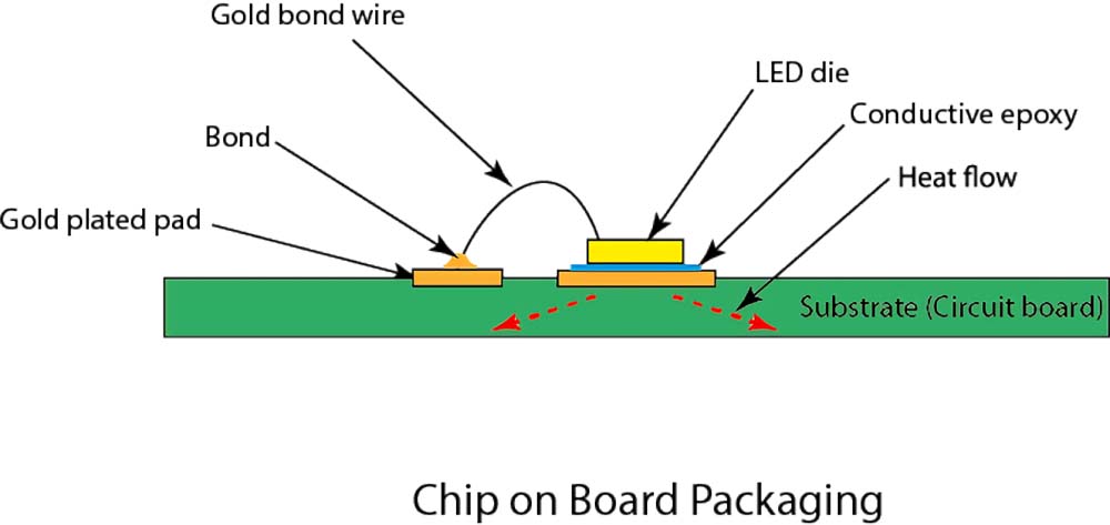
COB packaging technology
The core logic of COB packaging lies in “de-bracketing”. Its process flow can be summarized as follows:
Chip bonding: The LED chip is directly fixed on the PCB pad through conductive glue;
Welding test: Complete the electrical connection and performance test between chips;
Colloid packaging: Use epoxy resin glue to encapsulate the whole to form a protective layer.
With the integrated packaging method, COB packaging eliminates the traditional bracket structure and allows the chip to directly become part of the display unit. Taking the data of a leading manufacturer as an example, the first pass rate of its 2K integrated module has reached 30%, and the yield rate can be increased to more than 95% after rework.
SMD packaging technology
SMD follows the “single” packaging route:
Bracket bonding: fix the chip on the pad of the independent bracket;
Spectral taping: cut the taping after completing the performance test;
Patch assembly: the screen factory mounts the lamp beads to the PCB board.
The production data of an SMD manufacturer shows that its automated production line has a daily production capacity of 50 million lamp beads, but the single process leads to an increase in material turnover. For example: from the packaging factory to the screen factory, it needs to go through 5 intermediate links such as transportation and warehousing.
| Dimension | COB Packaging | SMD Packaging |
|---|---|---|
| Structural Complexity | Multi-chip integration, no independent support | Single LED with support structure |
| Production Process | Integrated production by packaging and display factory | Segmented production by packaging factory and display factory |
| Failure Repair | Repairable before encapsulation, bad points can be repaired individually | Failed LEDs require overall replacement |
Key difference COB Vs SMD screen
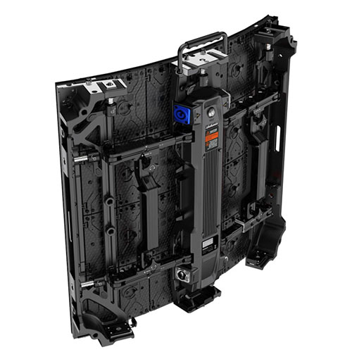
Packaging link
Cost advantage: COB can theoretically reduce the cost of bracket procurement, lamp bead taping, etc., but currently limited by the scale of production capacity, the cost per square meter is still 15-20% higher than SMD;
Quality control: SMD packaging factories can achieve a 99.9% factory yield through AOI equipment, while COB needs to cope with the thermal stress management challenges brought by integration.
Reflow soldering process
When SMD lamp beads are reflow soldered, the impact of 260℃ high temperature on the bracket solder pin cannot be ignored. Data from a certain laboratory shows:
The solder pin failure rate increases exponentially with the increase of temperature, and the failure risk increases by 3 times at 280℃;
COB completely avoids such risks because it has no solder pin structure, and its thermal shock test yield remains above 99.8%.
Ink color processing:
COB solution: achieve consistent ink color through colloidal formula optimization. A COB manufacturer has developed nano-level color paste dispersion technology, and the ΔE value is controlled within 0.8;
SMD solution: Relying on mask technology, but high-density lamp beads (below P1.2) are prone to color mixing, and the color gamut coverage is reduced by 12-15%.
Outdoor protection:
In the field of small pitch below P3.0:
COB module adopts a fully sealed design, and the combination of nano-coating + three-proof paint can achieve IP68 protection level;
SMD needs to glue each lamp bead solder pin separately, and the glue yield of a P2.5 project is only 82%, and the protection cost is 40% higher than COB.
Terminal reliability
In actual cases:
The COB screen of a subway hub has a bad pixel rate of only 0.0005% after 24 months of continuous operation;
The bad pixel rate of SMD screens in the same environment is 0.003%, and failures caused by bracket oxidation account for 65% of the total failures.
Industry chain ecology and market structure
Comparison of production models
COB vertical integration: full-process production from chips to modules, a leading manufacturer has achieved 72-hour fast delivery;
SMD division of labor and cooperation: the packaging factory and the screen factory operate independently, and a project was delayed by 15 days due to poor communication.
Cost structure analysis
Take P1.5 products as an example:
COB’s main costs are concentrated in equipment depreciation (35%) and colloidal materials (25%);
Among SMD costs, bracket procurement accounts for 20%, patch processing accounts for 18%, and warehousing and logistics accounts for 12%.
LED Technology evolution trend
COB direction:
Micro-pitch breakthrough: P0.7 product mass production has been achieved
Flexible display: Develop flexible PCB substrates
Intelligent detection: AI visual defect recognition system
SMD direction:
Bracket miniaturization: 0402 lamp beads are mature
Eutectoid welding: Improve heat dissipation performance by 30%
Spectral intelligence: Online color coordinate screening system
Future pattern prediction
Substitution dispute
From the market data:
In the field of indoor display, SMD still occupies more than 85% of the market share, but in scenarios such as high-end command centers, COB has achieved application breakthroughs.
Possibility of coexistence and development
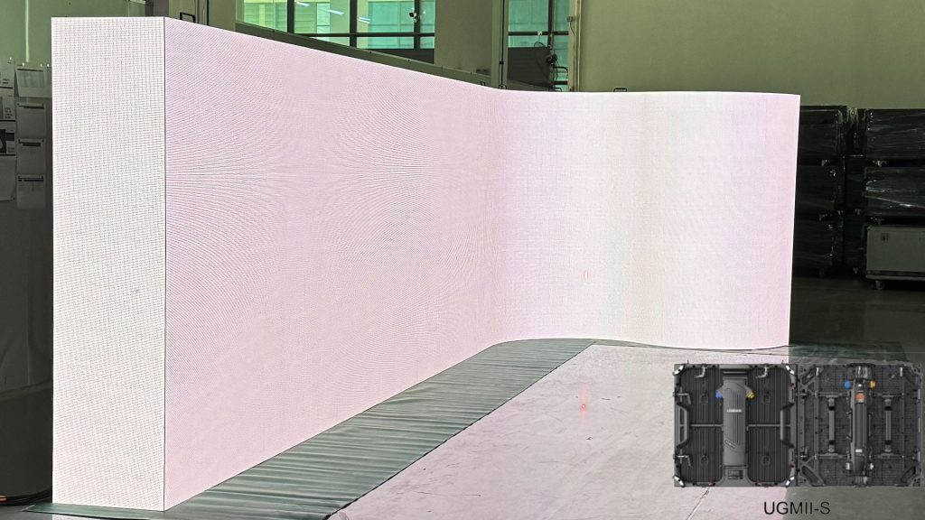
Scenario segmentation:
SMD: indoor conventional display, creative special-shaped screen
COB: indoor high protection, micro-pitch display
Technology integration:
Hybrid packaging solutions have appeared, such as SMD lamp beads + COB protection structure
Mini LED technology may give birth to new packaging forms
The ultimate decisive factor
Cost critical point: When the COB equipment investment recovery period is shortened to 3 years, a scale cost advantage will be formed
Technology iteration speed: If SMD breaks through the mass production technology of 0202 lamp beads, it can delay the market replacement process.
Ecological compatibility: COB needs to solve the matching problem with the driver IC, and SMD needs to improve the efficiency of supply chain collaboration.
| Aspect | COB Packaging | SMD Packaging |
|---|---|---|
| 1. Packaging Stage Analysis | ||
| Technical Difference | LED chips directly fixed on PCB, then encapsulated | LED chips mounted on a bracket, then encapsulated with sorting and cutting |
| Advantages | Simplified process, lower cost, improving yield | Mature technology, stable quality control |
| Disadvantages | Initially lower yield, improving over time | More complex process, higher cost |
| 2. Reflow Soldering Analysis | ||
| Technical Difference | No reflow soldering needed | Requires reflow soldering for LED attachment |
| Competitive Issues | Less competition due to lower production scale | Highly competitive, lower profit margins |
| Cost Issues | Lower cost due to simplified process | Higher cost as density increases |
| Reliability | No reflow defects, higher reliability | Risks of chip cracking, wire breakage |
| User-friendliness | Anti-static, impact-resistant, easy to clean | More fragile, sensitive to static and impact |
| 3. Black Surface Treatment | ||
| Technical Difference | Ink consistency issue mostly resolved | Relies on mask processing for uniformity |
| Evaluation | Both have stable reliability and similar costs | Both have stable reliability and similar costs |
| 4. Outdoor Protection Analysis | ||
| Technical Difference | Fully encapsulated, only PCB protection needed | Requires glue sealing for bracket pins |
| Competitive Issues | More advantages in P4-P3 levels | Strong competition, protection depends on bracket quality |
| Cost Issues | Stable protection cost, independent of density | Cost increases significantly with density |
| Reliability | No exposed pins, simpler protection, higher reliability | Glue sealing quality affects reliability |
| Protection Treatment | Curved surface, uniform coating, suitable for harsh environments | Sharp edges may cause coating dead zones |
Conclusion:
COB LED packaging has a great advantage in the field of small pitch and high-end display. However, due to the high maturity of SMD packaging and large production scale, SMD LED screens still dominate the market. However, with the advancement of COB LED packaging technology, we believe that in the future it is expected to surpass SMD packaging in more application. It will become the mainstream choice of the LED display industry.
